Made for the streets: Bosch’s silicon carbide (SiC) trench gate MOSFETs
Highly robust automotive semiconductors for demanding high-power applications

Robustness is essential for all components of electric vehicles. They must be able to operate for decades in demanding environments with exposure to internal and external factors. When it comes to silicon carbide (SiC) MOSFETs, the classic planar design is considered particularly robust and easy to manufacture thanks to its simple structure. But this technology is reaching the limits of its achievable performance. This is why Bosch has chosen an alternative route to satisfy the needs of automotive high-power applications: the production of trench gate MOSFETs based on SiC with high-precision vertical structures etched into the wafer material. Bosch has more than 20 years of experience in the field of automotive MOSFETs and SiC. Thanks to the innovative trench etching process, the power density of the chips is increased, while energy consumption is reduced at the same time. The design also offers an unmatched flexibility – allowing for continuous development in terms of robustness and efficiency.
Pushing intrinsic robustness
With the introduction of SiC trench gate MOSFETs, Bosch initiated a new era of SiC device technology: Unit cell size can now be significantly reduced, resulting in higher power densities. What’s more, Bosch’s dual-channel trench technology offers a solution for the technology’s Achilles’ heel. The vulnerable gate oxide is shielded very efficiently against high electric fields in the off-state of the transistor while achieving high reliability in the on-state by carefully controlling the gate oxide process.
This increases the robustness of the chip significantly, with a life span exceeding typical operating time. Additionally, the gate oxide has a very low threshold voltage drift, making it optimally suited for a variety of automotive-specific components. And Bosch does not stop here: the constant evolution of trench architectures is heading towards more compact designs, while shielding structures become more sophisticated. In maintaining the current pace of innovation, we expect the gate oxide reliability – and thus the level of robustness – in trenched devices to soon surpass that of planar SiC MOSFETs.
Better protection against external influences
Dealing with intrinsic electrical factors is one aspect of the robustness of SiC trench gate MOSFET devices. Another is how to handle the unavoidable cosmic rays that can lead to single-event burnouts. By optimizing the electric field shape and defining the breakdown voltage, Bosch is able to mitigate this impact thanks to the flexibility that comes with the trench architecture: The junction field-effect transistor (JFET) area below the trench can be tailored to reduce electric field peaks during blocking mode, leading to enhanced robustness. In consequence, overvoltage transients can be accepted for faster switching and lower switching losses.

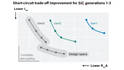
Short-circuit robustness is crucial for SiC MOSFETs. Unfortunately, it can influence the level of performance. Bosch has significantly improved the balance between specific on-resistance (equivalent to die size at a given current) and saturation current (equivalent to improved short-circuit robustness) with each generation. The effective result of the trade-off: SiC trench gate MOSFETs are capable of handling high currents on low chip areas and simultaneously ensure sufficient short-circuit robustness to meet the requirements of, for example, automotive traction inverter applications.

Full flexibility to maximize SiC semiconductor robustness
As one of the leading semiconductor suppliers for the mobility industry, Bosch is continuously investing in research and development. Backed by long-standing in-house expertise, application-adapted trench architectures are being explored to further improve SiC power devices and introduce new innovative features. Key trends include ultra-narrow pitch designs, the development of 3D structures, or trench superjunction devices. All these efforts share a common goal: lowest possible conduction losses and maximum robustness.


