APSM and other wet processes
APSM
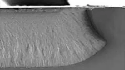
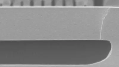
The APSM (Advanced Porous Silicon Membrane) process was developed by Bosch.
Bosch can generate a low density porous silicon. Optional can a subsequent anneal and epi silicon growth create a monocrystalline silicon membran on a defined and hermetically sealed cavity.

Porous layer:
- Porosity range: ~50 – 70%
- Thickness range: ~ 2 – 20µm
- Doping: ~ 2 – 3Ohm cm

Resulting cavity:
- Membrane thickness range: >= 4µm
- Cavity thickness range: ~ 2 – 10µm
- Cavity size tested: ~ 200 – 700µm
Benefits
- Fully CMOS compatible
- No bond frames needed > smaller chip sizes
- Monocrystalline Si membranes
- Full flexibility regarding size and shape of the membrane
Wet Cleans and Etch
All typical semiconductor Cleaning Procedures
- Wet bench incl. Marangoni dry
- FSI spray batch tool
- SAT spray etch backend and organic cleans
- Single wafer cleans
- SEZ
- Develop-removal of polyimide
- Specialties
Available Chemistry:
- Wet and organic
- HF, BHF, H2O2, H3PO4, SC1, SC2, various organic and metal etch chemistries (like EKC, DNP+, …), TMAH