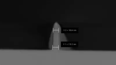
Photolithography
The fact, that MEMS and ASIC products are manufactured partly in the same fab, allows access to the existing ASIC processes, like DUV lithography, phaseshift technology, etc. Therefore i-line and 248 nm KrF are used in mass production for MEMS.

Features
- Phase shift technology
- CD down to 130nm line width
- Organic and anorganic BARC
- Various resist thickness up to 4µm in MEMS so far, higher possible
- Frontside-backside alignment
- Various photosensitive polyimides up to 12µm
- Mask aligner mit IR alignment und backside alignment