Dielectrica
SiN (Silicon Nitride)
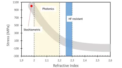
Silicon Nitride is an insulating material, which can be used for various applications. It is typically used in stoichiometric compostion as diffusion barrier. When the silicon content is increased, the silicon rich nitride “SiRiN” changes its material properties.
By adjusting the silicon content:
- the stress can be chosen
- the refractive index can be chosen, important for photonic devices
- the resistivity in HF etching can be achieved
This allows a wide range of additional applications in MEMS. The know-how regarding set up, operation and controlling SiRiN is crucial for success in many different running MEMS applications.
Capabilities
- Film thickness up to 1,400 nm
- SiN Stress tuning from –100 to + 1,000 Mpa
- Refractive index tuning from 1.98 to 2.50 (@780 nm measured)
- Applications:
- Stoichiometric Si3N4: passivation, diffusion barrier
- Silicon Rich Nitride (SiRiNi): electrical insulation layer, resistant to vapour-HF
- Medium refractive index: photonic layer
Specifications for standard photonic layer
- Film thickness: approx. 500nm
- Total range in production < 25 nm
- 1Sigma in production < 5 nm
- Refractive index: 2.09
- Total range in production < 0.01
- 1Sigma in production < 0.002

Other dielectrica
Methods
- Sputtering
- PE-CVD
- LP-CVD
- MoCVD
Materials
- TEOS
- Oxide incl. high temperature oxide
- Nitride
- Phosphorus doped and undoped Poly in various morphologies
Dry Etch for all above