Ion Beam Trim and CMP
Ion Beam Trim
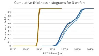
Ion Beam Trim allows to reduce the thickness variation of a certain film significantly, for example AlN and Si.
Thickness variation reduction by a factor of >20 is achieved
Requirements
Thin-Film thickness measured over the whole wafer. The number of measured points influence the trimming quality.

Capabilities
- Planarization of thin films
- Reduce variations of film thickness, improving the yield
- Surface roughness reduction / modification to improve adhesion of following depo steps
- Corrective etching and material modification depending on incoming film parameters
- State-of-the-art gas cluster ion beam (GCIB)
- Physical or chemically aided trimming
Materials
- Si, AlN, W, Ru, SiN, AlScN, and more.
-

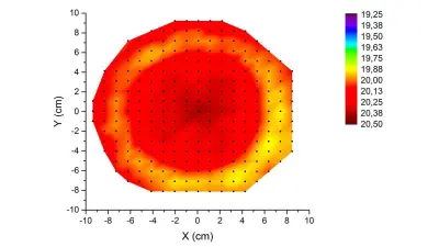
Ion beam trimming - wafer map before -

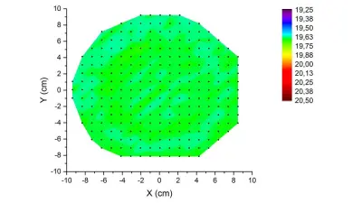
Ion beam trimming - wafer map after
CMP
Tool park including Ebara
Capabilities
- Oxide
- Poly-Silicon
- Tungsten
- Shallow Trench Isolation
- Copper
- Others optional
Clean after process
- In-situ clean with two clean stations roller brushes and brush pencil and drying
- NH4OH
- Megasonic
Other features
- 4 zones profile setup
- High selective processes
- Tungsten vs. Oxide
- Poly-Si vs. Oxide
- Si-Nitride vs. Oxide - Low and high planarization process for Poly-Silicon
- Endpoint detection optical, eddy current and motor current